Today, most manufacturers use Surface Mount Technology as a preferred method in manufacturing PCBs. However, hand/manual soldering is also useful when used effectively in the manufacturing process.
Read more to find out.
An easy-to-understand step-by-step guide to manufacturing small batches of box builds.
When a printed circuit board is manufactured certain important steps in the process make the boards reliable. Undoubtedly the components and processes are essential, while prompt and efficient communication is the key to building a PCB. At several stages of the process, decisions are to be taken by both the customer and the manufacturer to thereby design and develop a product that matches the requirements.
What are the steps generally involved in the process of building a product prototype (Box Build)?

Generally, the process for a fully functional box build begins with the customer providing data or specifications of the required product/prototype and communication continues until delivery.
Citing our recent project to highlight the process
For your better understanding, here’s our recent project as an example to outline the complete process of building a product prototype. The customer placed an order for a small batch of prototypes that would undergo a series of tests and evaluations.
A Step-by-step process involved in the process
1. Creating an Electrical Schematic Diagram


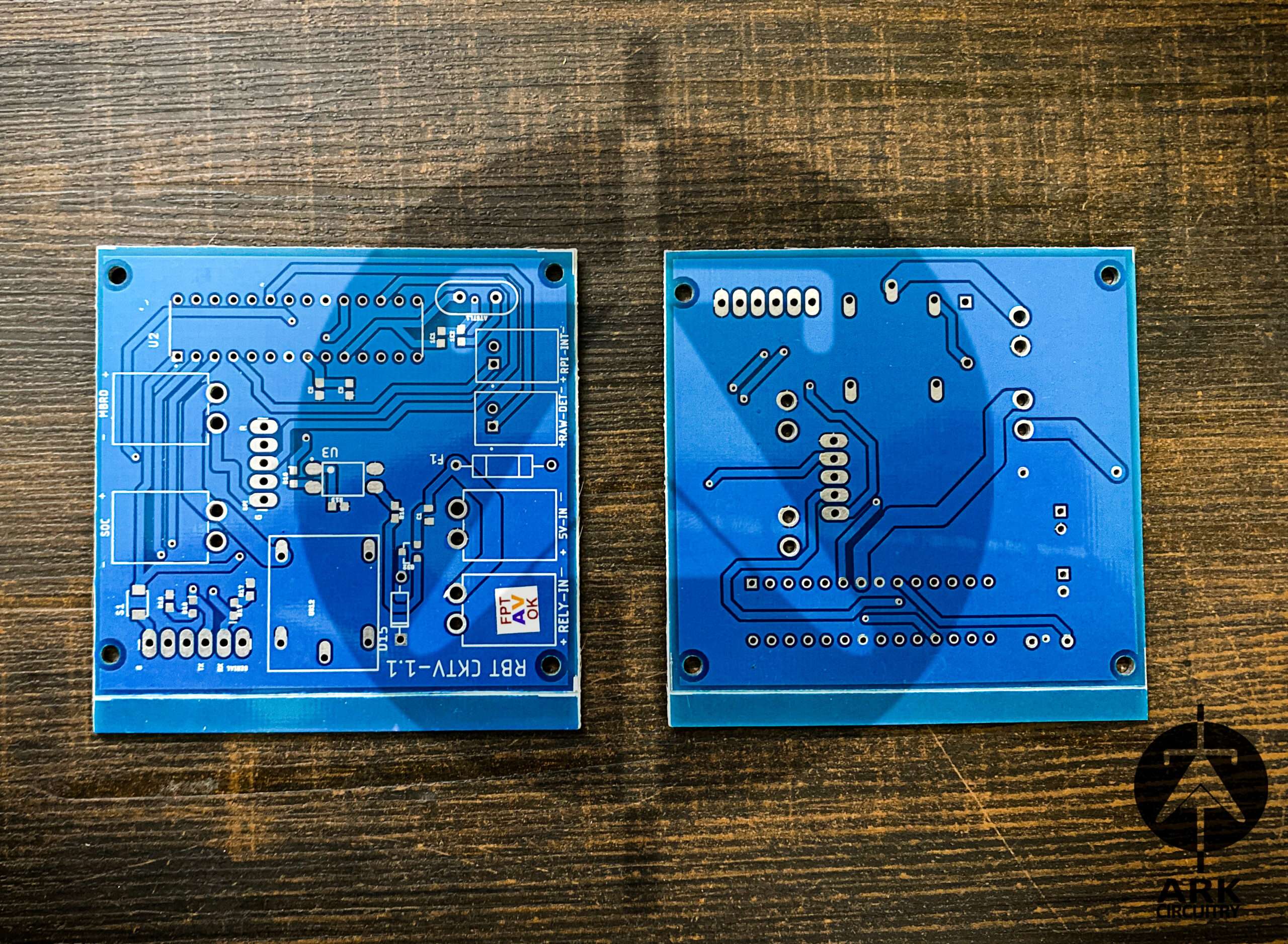
Firstly, the customer provided us with all the necessary details required to build the PCB. Then, the Electrical schematic diagram was designed for the circuit depending on the data provided. The schematic is very useful for building the PCB and equally valuable when troubleshooting. After that, the GERBER file is generated once the customer takes a final look before the PCB is sent for fabrication.
Once the board is fabricated, driven by the electrical requirements, the type and style of the components to be used were decided.
In general, although the manufacturer decides the configurations of the resistors, capacitors and diodes depending on the electrical requirements, the dimensions of the board requested by the customer influence the size of the components and the overall appearance of a finished PCBA.
2. Choosing components and the soldering process involved in PCBA


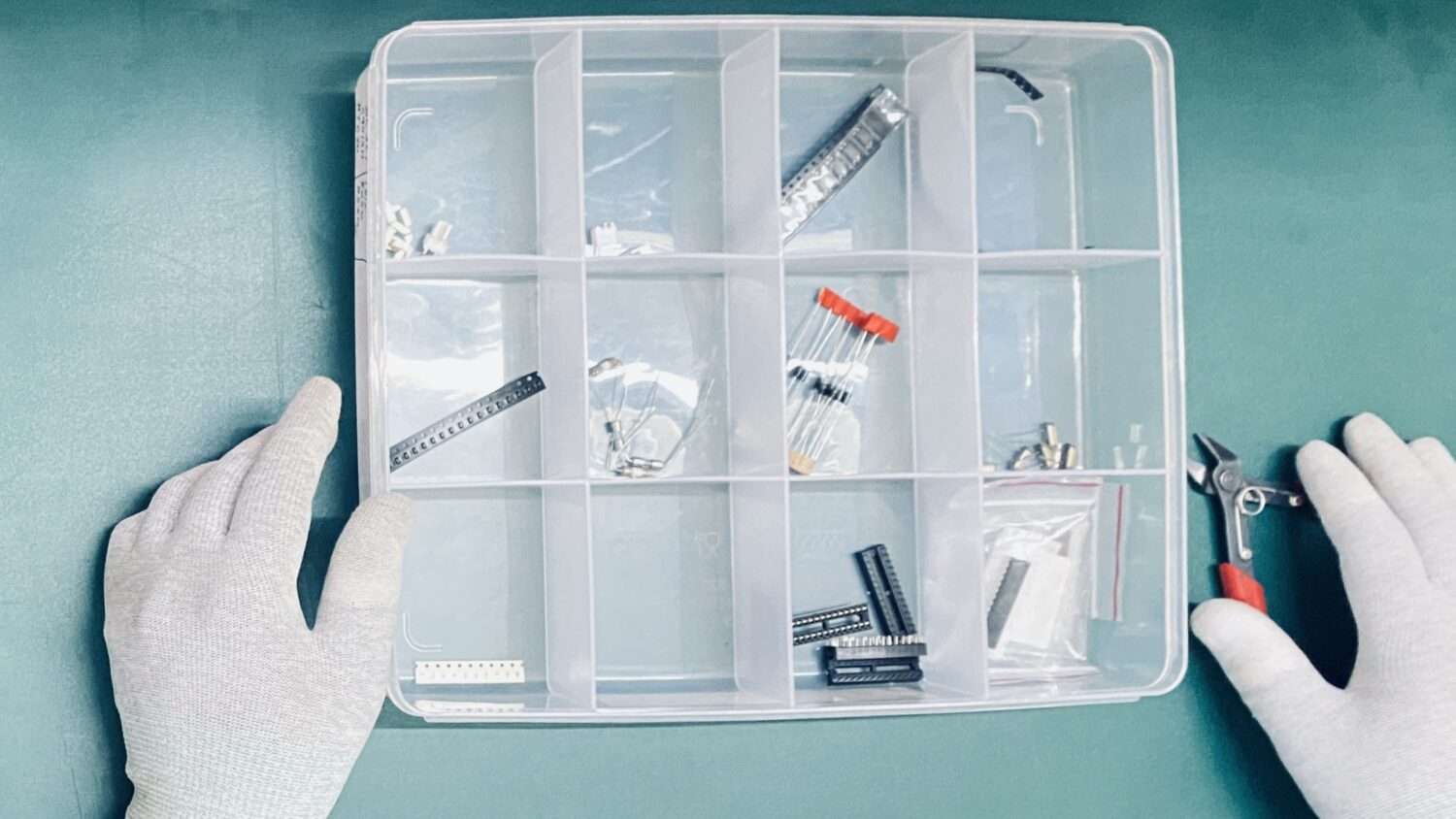
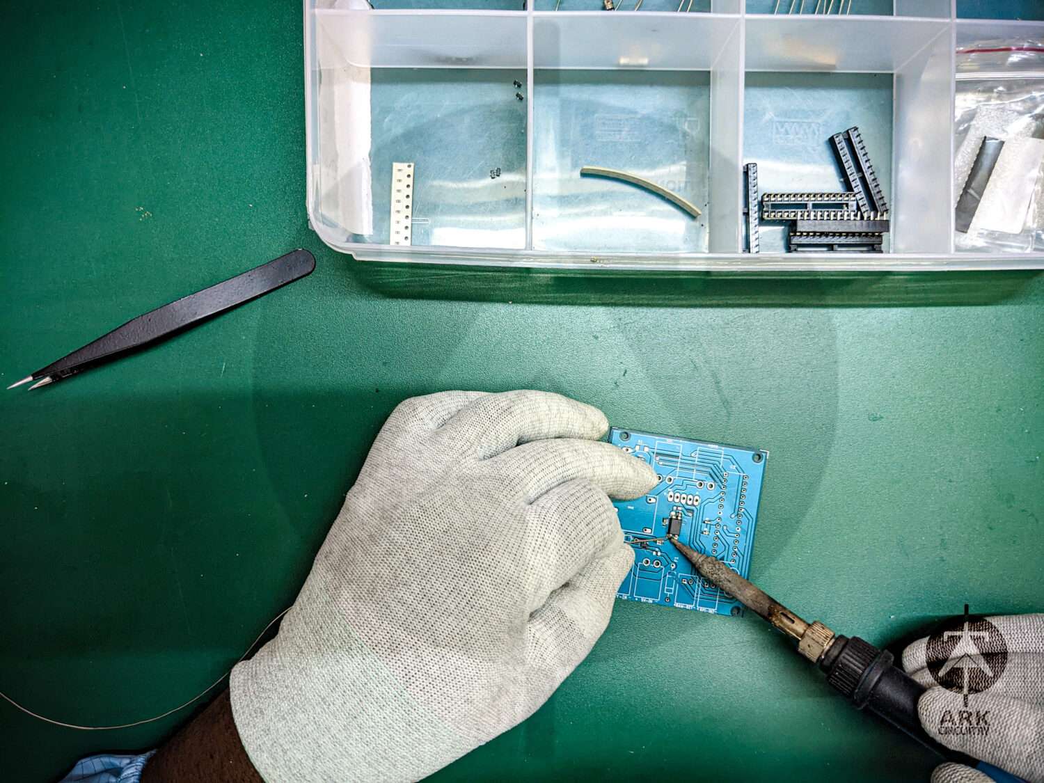
Next, through a volley of discussions, we decided to use a combination of through-hole and surface-mount components that were to be manually soldered on the fabricated PCB. A Bill of Materials (BOM) was generated and the components were procured by our procurement team.
Even-though through-hole is an older technology and a more modern technology such as the SMT (Surface Mount Technology) is preferred by manufacturers, manual soldering of components has its footing in certain areas of production.
Especially for prototyping circuit boards or for the production of a small batch of PCBs, manual soldering using through-hole or surface mount components or a combination is efficient. However, the soldering method also depends on the type of capacitors or resistors chosen.

3. Designing and Fabricating the 3D printed enclosure for the PCBA

Simultaneously, our design team began the process of designing the enclosure. It was designed according to the size of the board and its components. Using an FDM printer, Theta by IONIC3DP, the enclosure was 3D printed and built in-house.

4. Cleaning and testing the PCBA
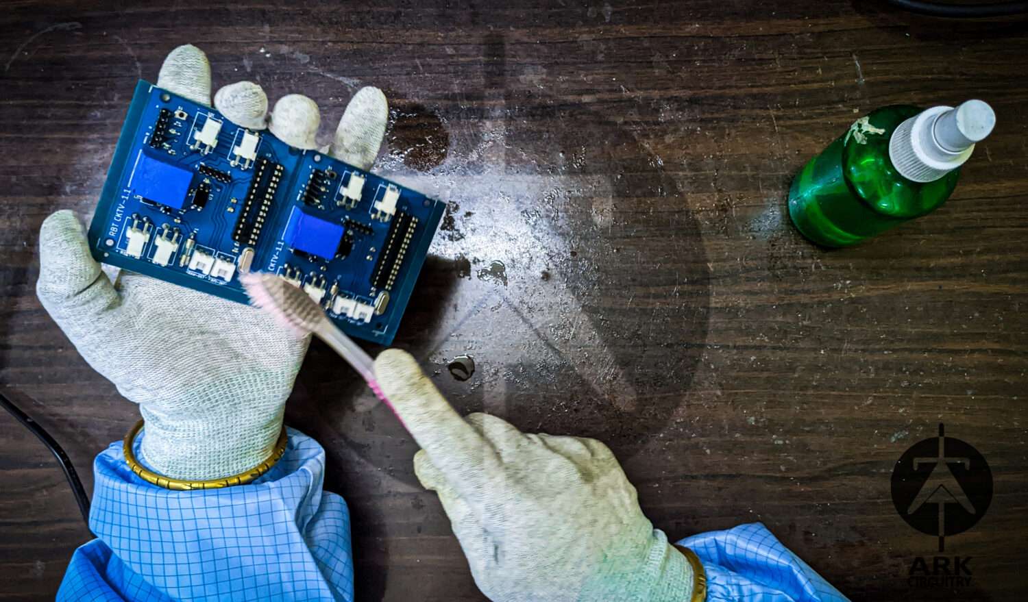
Once the PCB is assembled, each and every board is cleaned thoroughly. Before running basic checks and tests of functionality.
5. Installing the PCBA and completing the prototype
Finally, post testing the PCBA, the board is installed in the 3D-printed enclosure. Wiring and switches were added and the fully completed prototype was tested once again before packing it.
A batch of 120 fully assembled prototypes was completed, packed securely and shipped to the customer.
Ark Circuitry Ventures Is An EMS Provider And Specialise In Providing End-To-End Services That Can Be Tailor-Made To Meet Your Requirements.
Let’s talk for more information.
Call us on: +91 88259 58660
Mails us at: arkcircuitry@gmail.com
Visit us at: https://arkcircuits.com

