
Deciphering PCB Vias
Delve into the realm of PCB vias! This blog post dissects blind vias and through-hole vias, unravelling their differences, applications, advantages, and disadvantages.
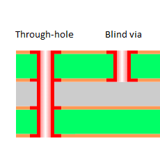
Vias are important conduits in printed circuit boards (PCBs) that establish connections between different layers. Blind vias and through-hole vias are essential elements with unique characteristics.
Blind Vias: Unlocking the Essentials
Blind vias are used to connect the outer layers of a PCB to one or more inner layers. These vias are especially useful for high-density designs and compact electronic devices.
Applications of Blind Vias:
- High-density interconnects in smartphones, tablets, and miniaturized electronics.
- Complex designs demanding intricate routing solutions.
Advantages of Blind Vias:
- Increased routing density, allowing for more compact designs.
- Improved signal integrity due to shorter connections.
- Reduced layer count, hence lower manufacturing costs.
Disadvantages of Blind Vias:
- Limited to specific layer connections.
- Demands precise drilling during fabrication, potentially increasing manufacturing complexity.
Through-Hole Vias: The Traditional Workhorse
Through-hole vias traverse the entire PCB, connecting all layers from top to bottom. While more conventional, they may not suit highly compact designs.
Applications of Through-Hole Vias:
- General PCB designs where reliability is crucial.
- Industries requiring robust and well-connected layers, such as automotive and aerospace.
Advantages of Through-Hole Vias:
- Enhanced reliability due to complete board penetration.
- Suitable for multilayer PCBs, ensuring stronger connections.
Disadvantages of Through-Hole Vias:
- Consumes significant space in dense designs.
- Complex manufacturing processes, potentially raise overall costs.
Blind Vias vs. Through-Hole Vias
Differences | Blind Vias | Through-Hole Vias |
Penetration | Penetrates only a portion of PCB layers | Traverses the entire PCB, top to bottom |
Layer Connectivity | Connects outer layers to inner layers | Connects all layers, offering full access |
Space Utilization | Offers increased routing density | Consumes more space, less ideal for density |
Complexity | Requires precise drilling for fabrication | Less complex manufacturing process |
Cost | Can reduce layer count, lowering costs | May increase manufacturing costs |
Application Suitability | Ideal for high-density designs | Suitable for general PCBs and robust connections |
Navigating the Viaduct
The decision to use either blind or through-hole vias depends on specific design requirements. Understanding their applications, trade-offs, and unique functionalities is crucial during PCB design and fabrication processes.
Get in Touch with Us
Our services cater to clients interested in manufacturing products in India, with a focus on reducing costs while enhancing both the quality and efficiency of their production process.
Looking to design or fabricate a PCB?
Talk to us to know more.
Mail us on arkcircuits@gmail.com
Call us at +91 9176418660.
Ark Circuitry is an integrated electronics design assembly and mass manufacturing service provider renowned for crafting end-to-end services that accurately align with your unique requirements. With our team of seasoned engineers committed to excellence, we provide reliable and high quality services!


