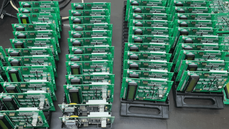
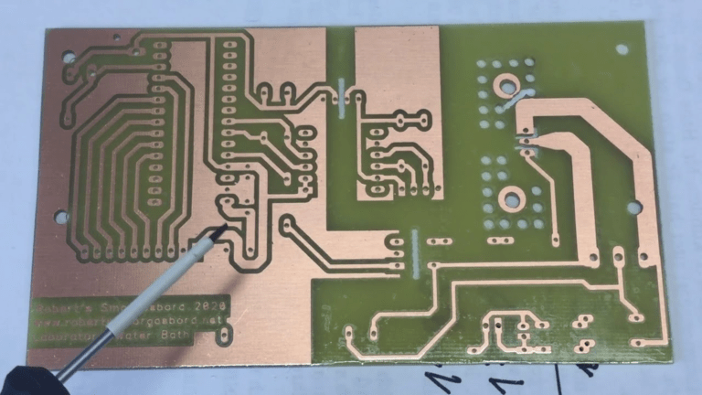
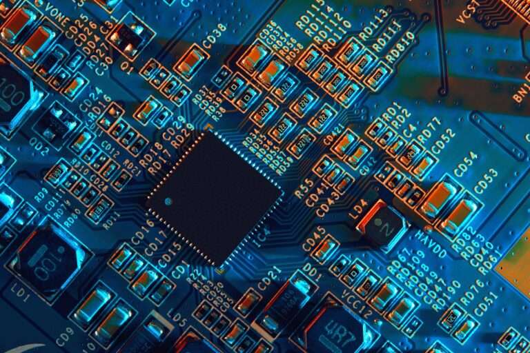
Printed Circuit Board (PCB) manufacturing is at the core of the electronics revolution. As the...
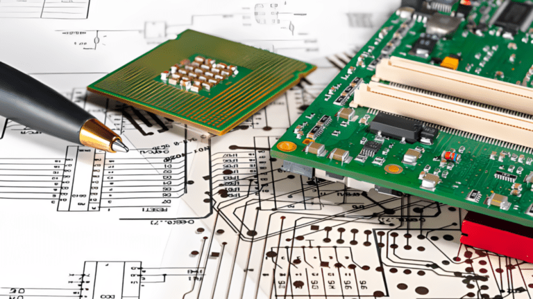
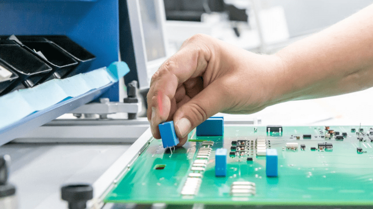
Choosing the right electronics manufacturing partner is a critical decision that can significantly...