The Advent of SMT
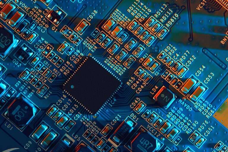
Surface Mount Technology emerged as a game-changer in the electronics industry, offering a more efficient and reliable method for mounting components onto PCBs. Unlike traditional Through-Hole technology, SMT allows components to be directly soldered onto the surface of the board, eliminating the need for drilled holes. This innovation has paved the way for more compact, lightweight, and high-performing electronic devices.
Miniaturization: The Drive Towards Smaller Devices
One of the most significant impacts of Surface Mount Technology is the ability to miniaturize electronic components. SMT components are much smaller than their Through-Hole counterparts, enabling designers to pack more functionality into a smaller space. This miniaturization has been crucial for the development of modern gadgets such as smartphones, wearables, and other portable devices, where space is at a premium.
Enhanced Performance: Speed and Efficiency
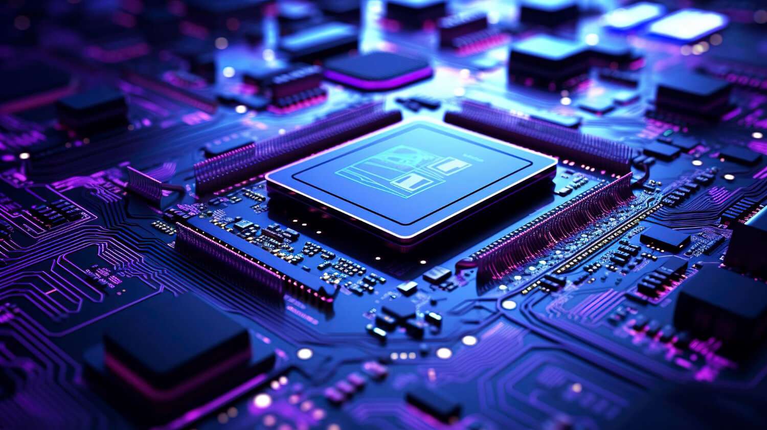
Surface Mount Technology enhances the performance of electronic devices by reducing the length of the electrical paths. Shorter paths mean less signal interference, lower resistance, and improved electrical performance. Consequently, SMT components facilitate faster signal transmission and higher processing speeds, making them ideal for high-frequency and high-performance applications.
Design Flexibility: Unleashing Creativity
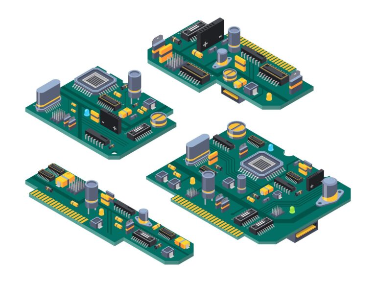
The flexibility offered by Surface Mount Technology has unleashed a new wave of creativity in PCB design. SMT allows components to be placed on both sides of the PCB, maximizing the use of available space. This dual-sided placement capability, combined with the smaller size of SMT components, provides designers with more freedom to create complex and innovative circuit designs.
Cost Efficiency: Streamlined Production
Surface Mount Technology has made PCB production more cost-efficient. SMT supports automated assembly processes, reducing labor costs and increasing production speed. The smaller size of SMT components also means less material usage, which translates to lower production costs. Additionally, the ability to place more components on a single PCB reduces the number of boards required, leading to further cost savings, especially in high-volume manufacturing.
Reliability and Durability: Building Robust Devices
Surface Mount Technology contributes to the reliability and durability of electronic devices. SMT components are soldered directly onto the PCB, providing better mechanical support and reducing the risk of physical damage. This method also ensures better heat dissipation, as components are in direct contact with the board, which acts as a heat sink. Furthermore, SMT components are less susceptible to vibration and shock, making them ideal for use in rugged and harsh environments.
The Future of PCB Design: Embracing SMT
As technology continues to evolve, Surface Mount Technology will remain at the forefront of PCB design and manufacturing. The ongoing advancements in SMT, such as the development of smaller and more efficient components, will continue to drive innovation and set new benchmarks for performance and reliability. Embracing SMT is essential for staying competitive in the fast-paced electronics industry.
In conclusion, Surface Mount Technology has had a profound impact on modern PCB design. From enabling miniaturization and enhancing performance to offering design flexibility and cost efficiency, SMT has revolutionized the electronics industry. As we look to the future, the role of SMT in driving innovation and setting new standards for PCB design will only continue to grow.